Quartz, due to its high purity, high-temperature resistance, excellent chemical stability, and superior insulation properties, has important applications in both the photovoltaic and semiconductor fields. The details are as follows:
1. Applications in the Photovoltaic Field
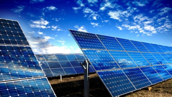
The core of the photovoltaic industry is the conversion of light energy into electricity through solar cells. Quartz’s applications primarily revolve around silicon wafer production:
1. Quartz Crucible
This is the most critical quartz component in photovoltaic silicon wafer manufacturing. During the Czochralski process (the Czochralski method), quartz crucibles are used to hold molten high-purity silicon. Their high purity prevents contamination of the silicon by impurities, and their high-temperature resistance (quartz melting point is approximately 1710°C) allows them to withstand the high temperatures of molten silicon (approximately 1410°C), ensuring the purity and quality of the single-crystal silicon ingots.
2. Quartz Ingots and Quartz Sheets
Some photovoltaic cells use quartz sheets cut from quartz ingots as substrates or masks in the thin-film deposition process. Their flatness and chemical stability aid thin-film growth.
II. Applications in the Semiconductor Industry
The semiconductor industry places extremely high demands on material purity and performance. Quartz is a key auxiliary material, used throughout multiple core stages of chip manufacturing:
1. Quartz Boats (Wafer Carriers)
Quartz boats are used to carry and secure wafers (silicon wafers) during processes such as wafer cleaning, diffusion, oxidation, and ion implantation. Their high purity (impurity levels typically below ppm) prevents wafer contamination, and their high-temperature resistance makes them suitable for high-temperature processes (such as the 800-1200°C environments found in oxidation furnaces).
2. Quartz Tubes and Windows
◦ Quartz tubes are core components of high-temperature furnaces (such as diffusion and oxidation furnaces). As the reaction chamber, they provide a clean, high-temperature environment for the wafers.
◦ Quartz windows are used in equipment such as photolithography and ion implantation as the light-transmitting window within the vacuum chamber. Their high light transmittance (especially in the UV range) meets the transmission requirements of photolithography light sources.
3. Quartz Reticle (Photolithography Aid)
In the photolithography process, high-precision quartz reticles are used to carry circuit patterns, which are then transferred to wafers via UV projection. Quartz requires extremely high flatness and dimensional stability.
4. Other Precision Components
Such components as quartz nozzles (used for gas distribution in etching or deposition processes) and quartz holders must meet the stringent cleanliness and corrosion resistance requirements of semiconductor processes.
Key Differences
• The photovoltaic industry has slightly lower quartz purity requirements than the semiconductor industry (photovoltaic quartz purity is typically above 99.9%, while semiconductors require above 99.99%), resulting in relatively lower costs.
• The semiconductor industry, due to the precision of chip manufacturing processes, places even higher demands on quartz purity, dimensional accuracy, and surface finish, making it the primary application for high-end quartz products.
In short, quartz, due to its unique physical and chemical properties, has become an indispensable key material in the photovoltaic and semiconductor industries, supporting the efficient production of silicon-based devices.