Looking at the entire semiconductor processing industry, it is inseparable from the support of key materials and components. For example, quartz materials and their products play an extremely important role in many aspects of the semiconductor industry due to their unique characteristics.
Quartz Crucible
Quartz crucibles have the advantages of high purity, strong temperature resistance, large size, high precision, and good heat preservation. Especially in the process of silicon crystal growth, the quartz crucible has become an irreplaceable key component!
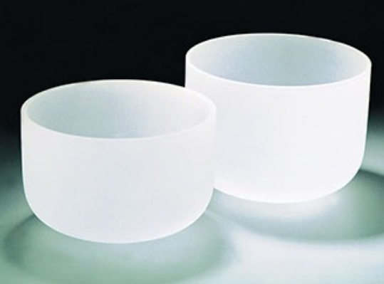
It should be noted that, according to different preparation processes and uses, quartz crucibles are divided into arc quartz crucibles and quartz ceramic crucibles. The arc quartz crucible is mainly used for Czochralski monocrystalline silicon, which is manufactured by the arc method (that is, used in the semiconductor field). method.
Monocrystalline silicon is an indispensable semiconductor material in the manufacture of large-scale integrated circuits. With the improvement of circuit integration, ultra-large-scale integration has developed rapidly. At present, the mainstream silicon wafer has reached 300mm, and 400mm monocrystalline silicon has also been successfully developed, and industrialization is just around the corner.
As we all know, large-diameter single crystal silicon (above 200mm) is basically produced by the Czochralski (CZ) method. It takes more time and more resources to grow such a large-sized silicon crystal. The crystal growth success rate is very important. During the growth of Czochralski silicon crystals, dislocation-free single crystal growth can fail due to various reasons, resulting in a great loss of resources and time. There are many reasons for the failure of the growth of dislocation-free single crystal products. Under the conditions that the current Czochralski silicon single crystal furnace and its thermal field design are stable and mature, the purity of the quartz crucible in direct contact with the silicon melt and its growth rate are very small. Cristobalite particles are generally considered to be one of the main reasons for the failure of the growth of large-diameter dislocation-free Czochralski crystals.
In other words, the quality of the arc quartz crucible is the main factor affecting the quality of Czochralski monocrystalline silicon. Therefore, the continuous improvement of the quality requirements for large-diameter single crystal silicon has put forward higher requirements for quartz products and related materials for semiconductor materials, such as quartz sand inspection, quartz sand purification, initial arc melting inspection, outer wall cleaning, cutting height, Chamfering, cleaning, coating, drying, final inspection, packaging, shipping, etc.
Etcher cavity, sample holder
The manufacturing of integrated circuit chips is inseparable from the etching process, and etching is one of the core technologies that determine the feature size of integrated circuits. The etching process refers to the transfer of the photoresist micropattern exposed by the pattern and on the surface of the semiconductor silicon wafer to the photoresist lower film material (usually SiO2, Si3N4 and the deposited metal layer and other films), that is, selective etching. The portion of the photoresist underlying material that is not masked by the photoresist is etched away. At present, the etching process mainly includes wet etching and dry etching.
For the etching of integrated circuit chip silicon wafers, whether dry or wet etching is used, it is necessary to use fluorine-containing gases (such as CF4, C2F4, C3F8, C4F8, CHF3, C5F8, CH2F2, etc.) or HF etching solutions. It is completed in a highly corrosive environment, which puts forward extremely stringent requirements for the etching reaction chamber and sample holder. In addition to high purity, it should also have excellent corrosion resistance, especially the dry etching process has a higher corrosion rate. quick. In the early days, Japan used materials such as alumina ceramics, yttrium aluminum garnet and aluminum nitride ceramics as auxiliary materials for etching, but the raw materials used in the manufacture of these materials were limited in purity and poor in machinability, and ceramic materials had crystal grains, which were corroded and fell off. It will pollute the semiconductor chip silicon wafer, thereby reducing the yield of the chip silicon wafer etching. In response to the above problems, manufacturers such as Japan and Germany have proposed to use quartz materials to make etching reaction chambers and sample holders.
However, ordinary quartz glass materials and even ordinary high-purity quartz glass are not competent. Because single-component high-purity quartz glass materials prepared by process technologies such as electrofusion, gas smelting, continuous melting, CVD or PCVD, will be rapidly corroded and destroyed in strong corrosive and high temperature environments such as fluorine-based gas or HF etching liquid. The application requirements of semiconductor etching cannot be met, so the corrosion-resistant quartz glass materials and products must be used in the integrated circuit etching process.
In this regard, companies such as Heraeus from Germany and Tosoh Quartz from Japan are relatively advanced in technology, and have the ability to mass-produce corrosion-resistant and durable quartz glass, which has been widely used in semiconductor etching and other processes. Japan Tosoh Quartz Co., Ltd. has studied the single doping of high-purity quartz powder with a certain atomic percentage of Al and element M (including more than one element in the periodic table Group 2A elements, Group 3A elements and Group 4A elements). or co-doping) to obtain a doped mixture, and then melt the doped mixture by electrofusion or gas smelting to obtain durable quartz glass. The principle of corrosion durability is that the boiling point or sublimation temperature of the fluoride of Al and element M The boiling point or sublimation temperature of SiF4 is high, so the oxides or fluorides of added elements are concentrated on the surface of quartz glass during etching in fluorine-based gas and plasma environment, which acts as a protective film, thereby improving the corrosion of quartz glass. Durability.
In addition to the above applications, as a key material and component, quartz products can be used in the whole process of semiconductor processing. For example, quartz tubes are used in semiconductor batch furnace processing as high-purity reaction chambers, gas or liquid inlets, or transport lines; quartz rods can be used to make boat hulls, wafer carriers, and susceptors; quartz plates can be used to make batch processing equipment Boats, susceptors, wafers and wafer carriers in the field. In monolithic processing equipment, sheets are used to make windows, gas distribution plates, shower plates, wafer carriers and carrier trays.