Silicon wafers are the cornerstone of semiconductor materials, which are first made into silicon rods by pulling a single crystal, and then cut into pieces. Since the number of valence electrons of silicon atom is 4 and the ordinal number is moderate, silicon has special physical and chemical properties and can be used in chemical, photovoltaic, chip and other fields. Especially in the field of chips, the semiconductor characteristics of formal silicon make it the cornerstone of chips. In the field of photovoltaics, it can be used for solar power generation. Moreover, the proportion of silicon in the earth’s crust reaches 25.8%, which is convenient to mine and highly recyclable, so the price is low, which further enhances the application scope of silicon.
Silicon – the cornerstone of chip materials
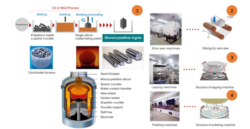
Silicon materials are divided into monocrystalline silicon and polycrystalline silicon according to the arrangement of the unit cells. The biggest difference between monocrystalline silicon and polycrystalline silicon is that the unit cell row of monocrystalline silicon is ordered, while polycrystalline silicon is disordered. In terms of manufacturing methods, polysilicon is generally formed by directly pouring silicon material into a crucible to melt, and then cooling it. Single crystal silicon is formed by pulling a single crystal to form a crystal rod (Czochralski method). In terms of physical properties, the characteristics of the two types of silicon are quite different. Monocrystalline silicon has strong electrical conductivity and high photoelectric conversion efficiency. The photoelectric conversion efficiency of monocrystalline silicon is generally around 17% to 25%, and the efficiency of polycrystalline silicon is below 15%.
Since photovoltaic silicon wafers have low requirements on parameters such as purity and warpage, the manufacturing process is relatively simple. Taking monocrystalline silicon cells as an example, the first step is to cut square and round. First, cut monocrystalline silicon rods into square rods according to the size requirements, and then round the four corners of the square rods. The second step is pickling, mainly to remove the surface impurities of the single crystal square rod. The third step is slicing, first paste the cleaned square bar and the work board. Then put the work board on the slicer and cut it according to the set process parameters. Finally, the single crystal silicon wafer is cleaned to monitor the surface smoothness, resistivity and other parameters.
Semiconductor wafers: Semiconductor wafers are more demanding than photovoltaic wafers. First of all, the silicon wafers used in the semiconductor industry are all monocrystalline silicon, in order to ensure the same electrical properties of each position of the silicon wafer. In terms of shape and size, monocrystalline silicon wafers for photovoltaics are square, mainly with side lengths of 125mm, 150mm, and 156mm. The single-crystal silicon wafers for semiconductors are round, with diameters of 150mm (6-inch wafers), 200mm (8-inch wafers) and 300mm (12-inch wafers). In terms of purity, the purity of single-crystal silicon wafers for photovoltaics requires a silicon content between 4N-6N (99.99%-99.9999%), but single-crystal silicon wafers for semiconductors are about 9N (99.9999999%)-11N (99.999999999%). The minimum purity requirement is 1000 times that of photovoltaic monocrystalline silicon wafers. In terms of appearance, the surface flatness, smoothness and cleanliness of silicon wafers for semiconductors are higher than those for photovoltaic silicon wafers. Purity is the biggest difference between single crystal silicon wafers for photovoltaics and single crystal silicon wafers for semiconductors.
Semiconductor Wafer Manufacturing Process
The development of Moore’s Law is the development of silicon wafers. Since silicon wafers for semiconductors are circular, semiconductor silicon wafers are also called “silicon wafers” or “wafers”. The wafer is the “substrate” for chip fabrication, on which all chips are fabricated. In the development of silicon wafers for semiconductors, there are mainly two directions of size and structure.
In terms of size, the development path of silicon wafers is getting larger and larger: in the early stage of integrated circuit development, 0.75-inch wafers were used. Increasing the wafer area and increasing the number of chips on a single wafer can reduce costs. Around 1965, with the introduction of Moore’s Law, both integrated circuit technology and silicon wafers ushered in a period of rapid development. Silicon wafers have gone through 4-inch, 6-inch, 8-inch and 12-inch nodes. Since Intel and IBM jointly developed 12-inch wafer chip manufacturing in 2001, the mainstream silicon wafer is 12-inch wafer, accounting for about 70%, but 18-inch (450mm) wafer has been put on the agenda.
In terms of structure, the development direction of silicon chips is becoming more and more complex: in the early stage of integrated circuit development, there was only one type of logic chip, but with the increasing number of application scenarios, logic chips, power devices, analog chips, digital-analog hybrid chips, flash/ Dram memory chips, radio frequency chips, etc. appeared one after another, making silicon wafers appear in different forms in structure. Now, there are three main ones:
PW (Polish Wafer): Polished wafer. Since the silicon wafers directly cut after pulling the single crystal are not perfect in terms of smoothness or warpage, they must first be polished. This method is also the most primitive way of processing silicon wafers.
AW (Anneal Wafer): Anneal wafer. With the continuous development of process technology, the feature size of transistors continues to shrink, and the shortcomings of polished wafers are gradually exposed, such as local lattice defects on the surface of silicon wafers, and high oxygen content on the surface of silicon wafers. To address these issues, annealing wafer technology was developed. After polishing, the wafer is placed in a furnace tube filled with inert gas (usually argon) for high temperature annealing. In this way, lattice defects on the surface of the silicon wafer can be repaired, and the oxygen content on the surface can also be reduced.
EW (Epitaxy Wafer): Epitaxy silicon wafer. As the application scenarios of integrated circuits continue to increase, the electrical characteristics of standard silicon wafers manufactured by silicon wafer factories can no longer meet the requirements of certain products. At the same time, the lattice defects reduced by thermal annealing cannot meet the demand for smaller and smaller line widths. This leads to epitaxial silicon wafers. The usual epitaxial layer is the silicon thin film. It is based on the original silicon wafer, using thin film deposition technology to grow a layer of silicon thin film. Since in silicon epitaxy, the silicon substrate exists as a mode of seed crystal, growing the epitaxial layer will replicate the crystal structure of the silicon wafer. Since the substrate silicon wafer is single crystal, the epitaxial layer is also single crystal. However, since it is not polished, the lattice defects on the surface of the grown silicon wafer can be reduced to a very low level.
Epitaxial technical indicators mainly include epitaxial layer thickness and its uniformity, resistivity uniformity, bulk metal control, particle control, stacking fault, dislocation and other defect control. At this stage, people have achieved high epitaxial layer silicon wafer quality by optimizing the reaction temperature of epitaxy, the flow rate of epitaxy gas, and the temperature gradient at the center and edge. Due to the needs of different products and technology upgrades, through continuous optimization of the epitaxial process, a high quality of epitaxial silicon wafers has now been achieved.
In addition, the current technology can generate epitaxial layers with resistivity doping elements and doping concentrations different from the original silicon wafers, which makes it easier to control the electrical properties of the grown silicon wafers. For example, an N-type silicon epitaxial layer can be formed on a P-type silicon wafer, thus forming a low-concentration doped PN junction, which can optimize the breakdown voltage and reduce the latch-up effect in subsequent chip manufacturing. . The thickness of the epitaxial layer generally varies according to different usage scenarios. Generally, the thickness of the logic chip is about 0.5 microns to 5 microns, and the thickness of power devices is about 50 microns to 100 microns due to the need to withstand high voltage.